High-performance lithium copper foil is one of the key materials for lithium-ion batteries and is closely related to battery performance. With the increasing demand for higher capacity, higher density, and faster charging in electronic devices and new energy vehicles, the requirements for battery materials have also been raised. In order to achieve better battery performance, it is necessary to improve the overall technical indicators of lithium copper foil, including its surface quality, physical properties, stability, and uniformity.
Analysis of microstructure using scanning electron microscope-EBSD technique
In materials science, the composition and microstructure determine the mechanical properties. Scanning Electron Microscope (SEM) is a commonly used scientific instrument for the surface characterization of materials, allowing observation of the surface morphology of copper foil and the distribution of grains. In addition, Electron Backscatter Diffraction (EBSD) is a widely used characterization technique for analyzing the microstructure of metallic materials. By configuring an EBSD detector on a field-emission scanning electron microscope, researchers can establish the relationship between processing, microstructure, and mechanical properties.
The figure below shows the surface morphology of electrolytic copper foil captured by the CIQTEK Field-emission SEM5000
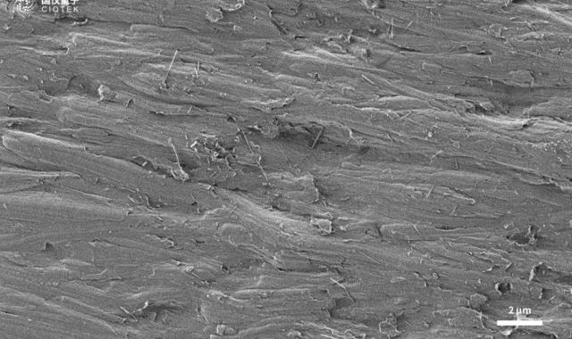
Copper Foil Smooth Surface/2kV/ETD
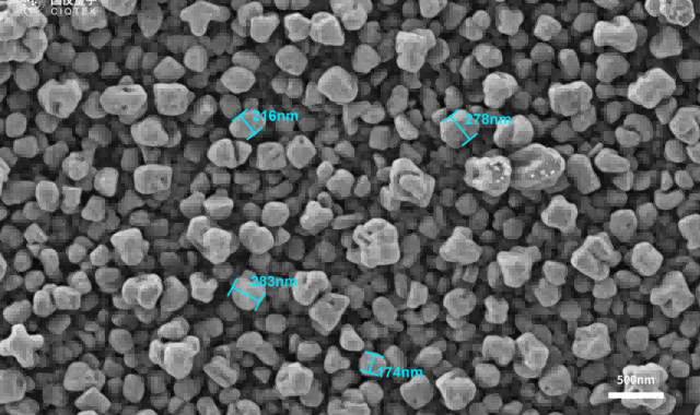
Copper Foil Matte Surface/2kV/ETD
When the sample surface is sufficiently flat, electron channel contrast imaging (ECCI) can be obtained using the SEM backscatter detector. The electron channeling effect refers to a significant reduction in the reflection of electrons from crystal lattice points when the incident electron beam satisfies the Bragg diffraction condition, allowing many electrons to penetrate the lattice and exhibit a "channeling" effect. Therefore, for polished flat polycrystalline materials, the intensity of backscatter electrons depends on the relative orientation between the incident electron beam and the crystal planes. Grains with larger misorientation will yield stronger backscattered electron signals and higher contrast, enabling the qualitative determination of grain orientation distribution through ECCI.
The advantage of ECCI lies in its ability to observe a larger area on the sample surface. Therefore, before EBSD acquisition, ECCI imaging can be used for rapid macroscopic characterization of the microstructure on the sample surface, including observation of grain size, crystallographic orientation, deformation zones, etc. Then, EBSD technology can be used to set the appropriate scanning area and step size for crystallographic orientation calibration in the regions of interest. The combination of EBSD and ECCI fully utilizes the advantages of crystallographic orientation imaging techniques in materials research.
By using ion beam cross-section polishing technology, CIQTEK obtains flat copper foil cross-sections that fully meet the requirements for ECCI imaging and EBSD analysis on scanning electron microscopes.
The figure below shows the characterization of electrolytic copper foil using the CIQTEK Field-emission SEM5000
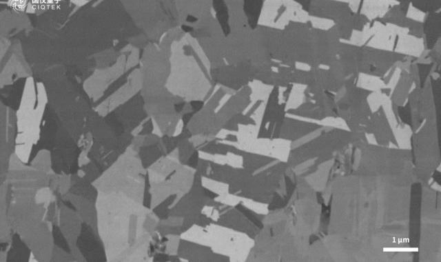
Electrolytic Copper Foil Cross-Section ECCI Image

Electrolytic Copper Foil Cross-Section Orientation Distribution
EBSD technology can not only characterize the grain size and dimensions but also reveal information about the material's texture type, grain boundary proportion, etc. By studying the microstructural evolution of electrolytic copper foil through ion beam sample preparation combined with SEM and EBSD techniques, it is of great significance to evaluate the differences in processing effects, further optimize the electrochemical properties of materials, improve battery cycle life, and even promote the development of lithium-ion battery technology.